
In the last decade, GaN demonstrated its superior performance in terms of output power, power densities and ruggedness for RF and Microwave as well as for switching applications.
Reliability issues are being progressively solved thus paving the way to a mature GaN technology.
High Power Amplifiers (HPAs) represent indeed the killer application of GaN technology, benefitting from high breakdown voltages and current densities, and leading to a 4X improvement in power densities as compared to more conventional GaAs realizations. Such performance in turn allows more compact circuits and hence a larger integration level.
Nevertheless, GaN robustness to impinging signals opens up the possibility to avoid the use of limiting sections in receivers, thus potentially improving receiver’s sensitivity for the same LNA performance.
The robustness and power handling of GaN-based single-pole multiple-throw switches completes the overall picture, allowing complete T/R module function replacement if the RF front-end is considered.
The 100 nm GaN technology (OMMIC D01GH GaN process) has been specifically developed to reach the same microwave performances than a conventional 130nm P-HEMT process (as provided e.g. by OMMIC itself, D01PH), but featured by a much higher output power.
As compared with other available GaN processes from the market, such 100 nm process has several unique features:
- 100 nm gate length and short gate/source distance, thus allowing high gain and low noise performance at millimetre waves
- in-situ passivation, allowing a lag not higher than achievable in P-HEMT processes with a quite short recovery time
- HR Silicon substrate, allowing a fully European supply chain and low costs for high volume production
- 12 V quiescent voltage bias for power and 3V-5V for noise applications, ensuring higher reliability of both passive and active devices, together with enhanced compatibility with existing systems.
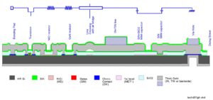
Cross-sectional view of the 100 nm GaN HEMT MMIC process by OMMIC
The process has complete MMIC features, with 2 levels of interconnection, high- and low-density MIM capacitors, two types of resistors, high power switch device, air-bridges and via holes through the Si substrate. It is documented in a design manual, and Design Kits are available for most popular circuit design packages.